Opus: Difference between revisions
| (14 intermediate revisions by the same user not shown) | |||
| Line 1: | Line 1: | ||
This is an analysis/reverse engineering review of the Opus BT-C3100 v2.2 4-slot Li/Ni battery charger/tester. | This is an analysis/reverse engineering review of the Opus BT-C3100 v2.2 4-slot Li/Ni battery charger/tester. | ||
[[File: | [[File:Opus_internal.jpg|thumb|right|Internal picture of the Opus tester.]] | ||
==List of Features== | ==List of Features== | ||
| Line 8: | Line 8: | ||
* Max Current (Charge): 2A (outer 2 slots simultaneous max, otherwise 1A) | * Max Current (Charge): 2A (outer 2 slots simultaneous max, otherwise 1A) | ||
* Max Current (Discharge): 1A | * Max Current (Discharge): 1A | ||
* Efficiency: | * Efficiency: 64.4% (charging, single slot at 2A, 3.8V) | ||
* Modes: Charge, Discharge, Discharge Test (C/D/C), Quick Test (IR), Discharge Refresh (10 cycles) | * Modes: Charge, Discharge, Discharge Test (C/D/C), Quick Test (IR), Discharge Refresh (10 cycles) | ||
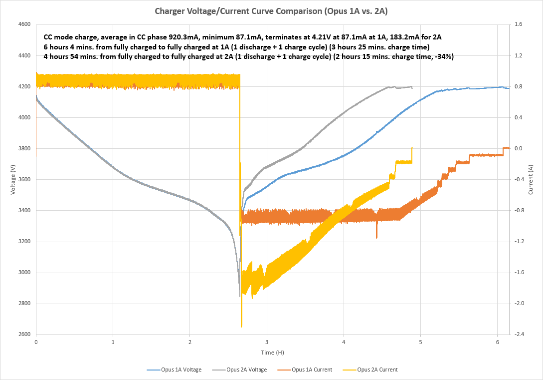
* 6-7mA current resolution (4 digits), 10mV voltage resolution (3 digits), 1.64Hz update rate | |||
[[File:1a-vs-2a_chargetest_opus.png|thumb|center|400px|1A and 2A charge/discharge curves for the Opus.]] | |||
==Electronics== | ==Electronics== | ||
| Line 19: | Line 18: | ||
A simplified schematic of the buck converter that charges the battery from a 12V supply is shown in the thumbnail below: | A simplified schematic of the buck converter that charges the battery from a 12V supply is shown in the thumbnail below: | ||
[[File: | [[File:Opus_charge_simple.png|thumb|center|400px|Simplified charging circuit schematic for the Opus.]] | ||
The input is decoupled with a 1000uF/16V electrolytic capacitor, plus 10uF of MLCC for each cell. The charger consists of a EUP3484 340kHz 3A synchronous buck converter, which steps down the 12V to either 3.273V (in Ni* battery mode) or 6.326V (in Li* battery mode), with a 15uH inductor and 220uF 10V electrolytic output capacitor. This is switched through an AO3419 P-channel MOSFET rated for up to 3.5A drain current, <102mOhm resistance at 4.5Vgs, and up to 1.4W power dissipation. This ~20Hz PWM switched output is then fed through an SS34 schottky diode (3A, 40V, 0.4Vf at 2A), and 2 0.12 Ohm current sense resistors in parallel to the battery positive terminal. | |||
Charge is terminated when the voltage exceeds 4.21V at 87mA average constant current (in 1A charge mode) or 18xmA average constant current (in 2A charge mode). | |||
===Resistor Discharger=== | ===Resistor Discharger=== | ||
A simplified schematic of the circuit that discharges the battery is shown in the thumbnail below: | A simplified schematic of the circuit that discharges the battery is shown in the thumbnail below: | ||
[[File: | [[File:Opus_discharge_simple.png|thumb|center|400px|Simplified discharger circuit schematic for the Opus.]] | ||
The battery positive goes through 2 0.12 ohm current sense resistors in parallel, through an SS34 schottky diode (3A, 40V, 0.4Vf at 2A), and into 6 5.1 ohm resistors in parallel (0.85 ohms equivalent), switched through an AO3400 N-channel MOSFET rated for up to 5.8A drain current, <33mOhm resistance at 4.5Vgs, and up to 1.4W power dissipation. The PWM rate for the MOSFET is 20 Hz. The peak battery current for a 4.2V Li-Ion battery is approximately 4A pulsed, accounting for voltage drops in the diode, FET, and current sense resistors. | The battery positive goes through 2 0.12 ohm current sense resistors in parallel, through an SS34 schottky diode (3A, 40V, 0.4Vf at 2A), and into 6 5.1 ohm resistors in parallel (0.85 ohms equivalent), switched through an AO3400 N-channel MOSFET rated for up to 5.8A drain current, <33mOhm resistance at 4.5Vgs, and up to 1.4W power dissipation. The PWM rate for the MOSFET is 20 Hz. The peak battery current for a 4.2V Li-Ion battery is approximately 4A pulsed, accounting for voltage drops in the diode, FET, and current sense resistors. | ||
Discharge termination is when the Li-Ion battery reaches 2.70V at constant current. There is no rest period after discharge before charging begins. | Discharge termination is when the Li-Ion battery reaches 2.70V at constant current. There is no rest period after discharge before charging begins. | ||
===Microcontroller=== | ===Microcontroller=== | ||
| Line 40: | Line 37: | ||
===Opus Performance Evaluation=== | ===Opus Performance Evaluation=== | ||
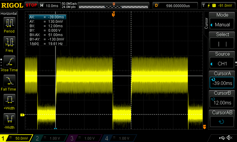
[[File:Opus-chargepwm-1A.png|thumb|center|400px|Opus charging current waveform at 1A; PWM at 19.6Hz from 0 to ~1.3A.]] | |||
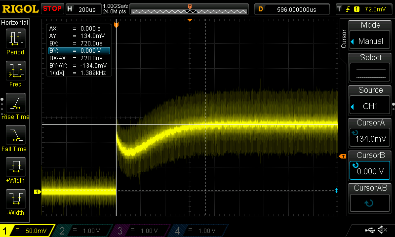
[[File:Opus-chargeramp-0-1A.png|thumb|center|400px|Opus charging current ramp up waveform to 1A; 720us settle time.]] | |||
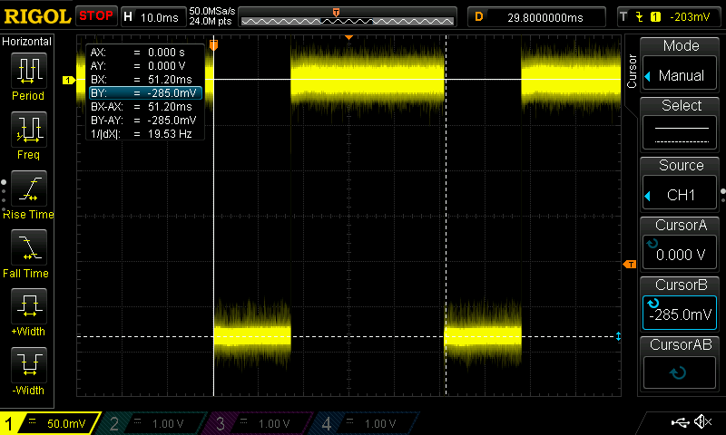
[[File: | [[File:Opus-dischargepwm-1A.png|thumb|center|400px|Opus discharging current waveform at 1A; PWM at 19.6Hz from 0 to ~2.85A.]] | ||
==BOM Cost Estimate== | ==BOM Cost Estimate== | ||
| Line 57: | Line 50: | ||
|- style="color:gray;text-align:left;" | |- style="color:gray;text-align:left;" | ||
| | |-} | ||
Latest revision as of 03:22, 10 December 2019
This is an analysis/reverse engineering review of the Opus BT-C3100 v2.2 4-slot Li/Ni battery charger/tester.
List of Features
- Voltage Range (Charge): 0-4.35V
- Max Current (Charge): 2A (outer 2 slots simultaneous max, otherwise 1A)
- Max Current (Discharge): 1A
- Efficiency: 64.4% (charging, single slot at 2A, 3.8V)
- Modes: Charge, Discharge, Discharge Test (C/D/C), Quick Test (IR), Discharge Refresh (10 cycles)
- 6-7mA current resolution (4 digits), 10mV voltage resolution (3 digits), 1.64Hz update rate
Electronics
Buck Converter (Charger)
A simplified schematic of the buck converter that charges the battery from a 12V supply is shown in the thumbnail below:
The input is decoupled with a 1000uF/16V electrolytic capacitor, plus 10uF of MLCC for each cell. The charger consists of a EUP3484 340kHz 3A synchronous buck converter, which steps down the 12V to either 3.273V (in Ni* battery mode) or 6.326V (in Li* battery mode), with a 15uH inductor and 220uF 10V electrolytic output capacitor. This is switched through an AO3419 P-channel MOSFET rated for up to 3.5A drain current, <102mOhm resistance at 4.5Vgs, and up to 1.4W power dissipation. This ~20Hz PWM switched output is then fed through an SS34 schottky diode (3A, 40V, 0.4Vf at 2A), and 2 0.12 Ohm current sense resistors in parallel to the battery positive terminal.
Charge is terminated when the voltage exceeds 4.21V at 87mA average constant current (in 1A charge mode) or 18xmA average constant current (in 2A charge mode).
Resistor Discharger
A simplified schematic of the circuit that discharges the battery is shown in the thumbnail below:
The battery positive goes through 2 0.12 ohm current sense resistors in parallel, through an SS34 schottky diode (3A, 40V, 0.4Vf at 2A), and into 6 5.1 ohm resistors in parallel (0.85 ohms equivalent), switched through an AO3400 N-channel MOSFET rated for up to 5.8A drain current, <33mOhm resistance at 4.5Vgs, and up to 1.4W power dissipation. The PWM rate for the MOSFET is 20 Hz. The peak battery current for a 4.2V Li-Ion battery is approximately 4A pulsed, accounting for voltage drops in the diode, FET, and current sense resistors.
Discharge termination is when the Li-Ion battery reaches 2.70V at constant current. There is no rest period after discharge before charging begins.
Microcontroller
The Opus BT-C3100 uses an unknown microcontroller that is wire bonded to the PCB, under a black epoxy blob.
Opus Performance Evaluation
BOM Cost Estimate
| EE Component | Cost | Source |


