CCR-HP: Difference between revisions
| Line 265: | Line 265: | ||
[[File:Ccr_both.png|thumb|right|The PCB layout (Gerber view from JLCPCB) for the CCR v1.0.]] | [[File:Ccr_both.png|thumb|right|The PCB layout (Gerber view from JLCPCB) for the CCR v1.0.]] | ||
This is the first revision of the CCR | This is the first revision of the CCR-HP. | ||
'''Errata:''' | '''Errata:''' | ||
* TO- | * TO-247 FETs Q2, Q4, Q5, Q6 footprints were reversed | ||
* Footprint for op-amps are incorrect | * Footprint for discharge feedback op-amps U3, U7, U8, U13 are incorrect (MCP6001 instead of MCP6001U style) | ||
* Footprint for bootstrap capacitor C1 is too small (needs to use 100V capacitor, 1210 size) | |||
* Pull-down for C1ON (discharge/charge enable protection FETs) R72 should be pull-up to default to off | |||
* Inverting/Non-inverting inputs to MCP6002 U11 are swapped | |||
====PCB Files==== | ====PCB Files==== | ||
Revision as of 22:41, 20 February 2020
This is a project to create a high power (200W target) DC load, with charging capability up to 84V, which when used in conjunction with computer software can graph data in real time to Thingspeak or InfluxDB/Grafana for analysis.
List of Features
Version 1
- Voltage Range (Charge): 0-84V
- Max Current (Charge): 10A (TBD)
- Max Current (Discharge, Regen): 10A (TBD)
- Max Current (Discharge, Resistive): 40A (TBD), 200W max power
- Min Current Readback Precision: 6mA (Lo range, -5-20A), 12mA (Hi range, -10-40A)
- Min Voltage Readback Precision: 2.3mV (Lo range, 0-9.46V), 23mV (Hi range, 0-94.6V)
- Sample Rate: 1 Hz (Reporting rate), 2 kHz (Loop/Integration rate)
- Efficiency: xx% (Buck/charge mode, average, 3A output), xx% (Boost/discharge mode, average, 3A output)
- Modes: Charge, Discharge (CC with voltage cutoff, CC-CV with current threshold cutoff), Power Supply (no cutoff below current threshold), Cycle (N times), IR measurement
Comparison to Other Cell Testers
A table comparing the features of some of these common testers is below:
| Feature | CCR-HP | PowerLab-8T | iCharger X8 | iCharger 4010Duo |
| Price | $149.99 (TBD) | $329.95 | $119.99 | $385.00 |
| Max Li-Ion s config | 20s (84V) | 8s (34.8V) | 8s (34.8V) | 10s (43.5V) |
| Max Balance Current | 0.38A** | 1A | 2A | 2.4A |
| Charge Current (Max) | 10A (TBD) | 40A | 30A | 30A |
| Discharge Power (Current) | 200W (40A) | 95W (8A) | 50W (15A?) | 200W (7A) |
| Regen Discharge Power (Current) | 840W* (10A) | 1350W (40A) | 1100W (30A) | 2000W (70A) |
- *Peak power with 20s pack, 24s buffer pack
- **With separate balancing board, resistive only
Thingspeak
Thingspeak is a website that allows users to send periodic data to a channel. Each channel can support 8 fields of data, e.g. voltage, current, temperature, etc.. The free version of Thingspeak, as of 3/10/19, allows users to have up to 4 channels, and can send data at a maximum rate of one "message" every 15 seconds, per channel. A message is a single http request, and can contain up to 8 fields. Updating the first 4 fields, then the second 4 fields counts as 2 messages, and is still limited to the 15 second "rule". Hence, it is best to update all 8 fields at once, to maximize the available bandwidth to Thingspeak. Note you can send data to 2 different channels at the same time, for up to 4 channels * 8 fields per 15 seconds of throughput.
To post to Thingspeak, the following format is used in an http request (example using wget): wget -q -O- "https://api.thingspeak.com/update?key=$KEY&field1=$CAPACITY&field2=$VOLTAGE&field3=$CURRENT&field4=$BTEMP&field5=$CTEMP"
In the case of the CCR, we are interested in using 2 channels per tester, one for real time status (voltage, current, temp, capacity) of each cell, and another for end of (discharge) cycle data for each cell. The real time channel should be updated once every 20s, with the combined data from slot 1 and slot 2 (if both cells are being tested simultaneously) combining both cells data into a single line/http request.
For the end of cycle channel, each cell's data can be sent asynchronously, but must not be sent within 20s of each other, otherwise the 2nd message may be dropped. Hence the code needs to check whether a message was sent in the last 20s before posting. If so, it will wait until the channel is not busy, then send.
Development
CCR-HP v1.0
This is a fully functional regenerative dual cell cycler which has been in use cycle testing a Re-volt 2.7AH 18650 vs Samsung 2.6AH 18650 for several months (over 500 cycles and xxxx hours of continuous operation as of 3/2/19). The board had to have several IO changes to resolve the USB errata mentioned in the Errata section. This board is connected to a ~3.6AH 2s buffer pack which is fitted with a 2s BMS and non-linear passive balancer consisting of 2 blue LEDs, one across each cell, which helps keep the pack balanced when it is at lower state of charge. It functions by draining more current exponentially with voltage above 3.3V, tending to keep both cells at the same voltage. The pack is kept at 7V minimum by a CC-CV buck converter fed from a 15W 12V power adapter.
The cycler's live operation can be followed here for the Samsung 26H cell: http://rev0.net/ts_samsung.html and here for the Re-volt cell: http://rev0.net/ts_revolt.html

Devices
| Hardware Version | HW Config | Slots | Serial Number | Status | Software Version |
| Prototype COTS | Specific | 1 | N/A | Disassembled | 0.5 |
| CCR v1.0 (Regen only) | v1.0 | 2 | N/A | Functional, using 2s2p LG D1 buffer pack | 0.5-10252018 |
| CCR v1.0 Dev | Specific | 1 | N/A | Functional | 0.x |
| CCR v1.0 Dev+Buck | Specific | 1 | N/A | Functional | 0.5-11152018 |
| CCR v1.0 Dev+3A Buck | Specific | 1 | N/A | Needs MCU replacement | 0.x |
| CCR v2.0 Cost Down | HW_2_0, V_1S | 2 | N/A | Functional, 5V supply, with Phizicks | 2.0-06262019 |
| CCR v2.0 | HW_2_0, V_1S | 2 | 001 | Functional, 12V supply, with Generic | 2.0-11132019 |
| CCR v2.4 | HW_2_0, V_2S | 2 | 002 | Functional, 12V supply | 2.0-11132019 |
| CCR v2.3 10uH | HW_2_0, V_2S | 1 | 001 | Needs FET/Driver replacement, 12V supply+3s2p HP LiPo | 2.0-11132019 |
Heatsink Sizing
The cooling solution for the 2 MOSFETs that make up the discharging circuit is a 100x40x20mm aluminum extruded heatsink with 11 fins, and a 5V 40x40x20mm fan. Results are as follows (tested at ~21 C ambient):
- 4A 4.2V (16.8W) (2A x2) - 65 C max on FET body, approx. 71.3 C Tj
- 5A 4.2V (21W) (2.5A x2) - 75 C max on FET body, approx. 82.9 C Tj
- 6A 4.2V (25.2W) (3A x2) - 84 C max on FET body, approx. 93.5 C Tj
- 7A 4.2V (29.4W) (3.5A x2) - 93 C max on FET body, approx. 104 C Tj
- 4A 4.2V (16.8W) (4A x1) - 79 C max on FET body, approx. 91.6 C Tj
- 5A 4.2V (21W) (5A x1) - 93 C max on FET body, approx. 108.8 C Tj
Electronics
Buck Converter (Charger)
A simplified schematic of the buck converter that charges the 18650 from a 6-12V supply is shown in the thumbnail below:

The input is decoupled with 220uF of electrolytic capacitors for each cell, total 440uF, plus 10uF of MLCCs for each cell. This is switched through an NCE30P12S P-channel MOSFET rated for up to 12A drain current, <25mOhm resistance at 4.5Vgs, and up to 3W power dissipation. Current is then supplied through 2 SS54 diodes in parallel during the off state, for up to 10A rated current at ~0.4Vf at 3A. The output is then filtered through another 440uF of electrolytic capacitors plus 10uF of MLCC.
Boost Converter (Discharger, regenerative)
A simplified schematic of the boost converter that discharges the 18650 into a 6-8.4V buffer pack is shown in the thumbnail below:

The input is decoupled with 440uF of electrolytic capacitors plus 10uF of MLCC. This is switched to ground through an AO4406AL N-channel MOSFET rated for up to 13A drain current, <15.5mOhm resistance at 4.5Vgs, and up to 3W power dissipation. Current is carried through 2 SS54 diodes in parallel during the off state, for up to 10A rated current at ~0.4Vf at 3A. The output is then filtered through another 440uF of electrolytic capacitors plus 10uF x2 of MLCC.
CCR v1 Performance Evaluation


Constant Current Load (v2 Discharger, resistive)
A simplified schematic of the MOSFET + Op-Amp based circuit that discharges the 18650 is shown in the thumbnail below:

The input is decoupled with 440uF of electrolytic capacitors plus 10uF of MLCC. This is discharged to ground through an IRF3710 N-channel MOSFET rated for up to 57A of drain current, ~17mOhm resistance at 4.5Vgs, and up to 200W power dissipation (limited to 21W for single channel based on 100x40x20mm heatsink + 40x40x20mm fan). Current measured across a 10mOhm shunt resistor is fed back to the Op-amp which compares it to a filtered PWM output from the STM32 microcontroller to control the current of the 18650. There is an additional input to the Op-amp to override the feedback and bias the MOSFET off (e.g. during charge or disconnected modes). The original circuit is credited to Youtuber VoltLog (video link) who reverse engineered a commonly sold "60W" constant current load and provided a detailed schematic. This circuit was prototyped on a proto board and then made into 2 standalone PCBs, one for through-hole kit form, and another small version using SMD parts.
Microcontroller
The CCR uses an STM32F103C8T6 microcontroller in the form of a "blue pill" board, which includes crystals, header pins, USB plug, and other supporting circuitry, and allows for the MCU to be swapped out in case of damage. Critically, the STM32F103 supports 8 12-bit ADC channels with fast read rate, 6 PWM channels operating at up to 360 kHz with 100 step PWM resolution, and built in USB PHY for communicating via virtual COM port to the PC.
CCR v2.6
This was a hardware change to use a 2-stage lower inductance buck (buck converter with 48.4uF/10uH/49.2uF followed by 1.5uH/22uF filter stage, compared to the original 460uF/60uH/450uF single buck converter, which showed promising improvements in voltage/current ripple in LTspiceIV simulation. Power supply and charging modes showed improvement to current/voltage ripple as expected, but reduced stability (the lower inductance/capacitance converter requires a higher loop bandwidth to maintain the same response). As soon as the cycle changed to internal resistance test (discharge mode, 6A peak) the low side switching FET and FET driver blew. The cycler was repaired with a new set of FETs + driver and tested functional. It was determined the ripple voltage at the switching node was high, and a snubber was added (20nF + 13.5 Ohm) to reduce this peak voltage. The snubber was simulated to dissipate approximately 0.7W, and reduced the ringing peak voltage to ~20V peak.


Calibration Procedure
When a device is initialized with a new microcontroller, there are no parameters stored to internal memory, thus initial values based on ideal values will be used.
Reference Voltage
The reference voltage used for the zero point of the two current shunt amplifiers and for scaling against supply voltage drift must first be measured, preferably with a 20000 count multimeter or better to get the 5 significant figures of the calibration value.
- Measure voltage from pin A5 to ground pin on the Blue Pill board.
- Take the decimal portion of the value (e.g. 6544 for 1.6544V measured.
- Write this value to memory using the following command: "tw a0 d6544", where the number after "d" is the value recorded in the previous step.
Output Voltages
The output voltage of the charger must be measured to account for resistor variation in the 4-wire Op-amp circuit for voltage measurement, preferably with a 6000 count multimeter or better to get the 4 significant figures of the voltage value.
- Start the slot to be measured to 4.2V output using the power supply mode (e.g. "p1" for slot 1, 4.2V output)
- Measure voltage across the cell holder of the slot to be measured.
- Take the voltage value in mV (e.g. 4302 for 4.302V measured.
- Write this value to memory using the following command: "tw aX d4302", where the number after "d" is the value recorded in the previous step, and "X" is the slot tested (1 or 2).
Output Currents
The charger/discharger current must be measured to account for shunt resistor and shunt amplifiers gain variation in the current measurement circuit, preferably with a 2000 count multimeter or better to get the 4 significant figures of the current value.
- Connect a power supply or cell negative to the negative side of the slot to be measured.
- Connect a multimeter set to current mode, 2A range (or equivalent to get a reading of 1A), from the positive of the cell/power supply to the positive cell holder terminal.
- Ensure the cell/power supply is 3.7-4.2V.
- Start the slot to be measured to discharge mode, 1A current, using the following command: "d1 i1000" for slot 1, 1A
- Measure current through the multimeter for the slot to be measured.
- Take the current value in mA (e.g. 1053 for 1.053A measured.
- Write this value to memory using the following command: "tw aX d1053", where the number after "d" is the value recorded in the previous step, and "X" is the slot tested + 2 (3 or 4).
Input Voltage
The charger/discharger input voltage must be measured to account for voltage divider resistor variation, preferably with a 6000 count multimeter or better to get the 4 significant figures of the input voltage value.
- Connect a power supply set to 5.000V to the input of the CCR
- Get the input voltage value using the status "s" command
- Take the input voltage value in mV (e.g. 4953) output by the command (first value after "4," message)
- Write this value to memory using the following command: "tw a5 d4953", where the number after "d" is the value recorded in the previous step.
Hardware Revisions
Revision 1.0


This is the first revision of the CCR-HP.
Errata:
- TO-247 FETs Q2, Q4, Q5, Q6 footprints were reversed
- Footprint for discharge feedback op-amps U3, U7, U8, U13 are incorrect (MCP6001 instead of MCP6001U style)
- Footprint for bootstrap capacitor C1 is too small (needs to use 100V capacitor, 1210 size)
- Pull-down for C1ON (discharge/charge enable protection FETs) R72 should be pull-up to default to off
- Inverting/Non-inverting inputs to MCP6002 U11 are swapped
PCB Files
Eagle schematic/board files and gerber files can be found here: https://github.com/jkenny23/CCR-HP-HW
Enclosure
The enclosure for the CCR v2.0 was created in Fusion 360 and is made up of x pieces which can be 3D printed and assembled with M3 screws.
Here are the Fusion 360 files for the CCR v2.0 enclosure: http://rev0proto.com/files/tbd.zip

Code
Full source code for the project can be found here: https://github.com/jkenny23/CCR_v2.0
EEPROM Map for Calibration Values
| EEPROM Address | Description | Typical Value |
| 0x0000 | Reference Voltage (Real Value - 1.0V) (mV*10) | 6500 |
| 0x0001 | Slot 1 Correction Voltage (Real Value) (mV) | 4200 |
| 0x0002 | Slot 2 Correction Voltage (Real Value) (mV) | 4200 |
| 0x0003 | Slot 1 Correction Current (Real Value) (mA) | 1000 |
| 0x0004 | Slot 2 Correction Current (Real Value) (mA) | 1000 |
| 0x0005 | Input Voltage Correction Value (Reported Value) (mV) | 5000 |
Videos
<HTML5video type="youtube" width="400" height="300" autoplay="false">1SHY4jAfTcM</HTML5video>
Photos
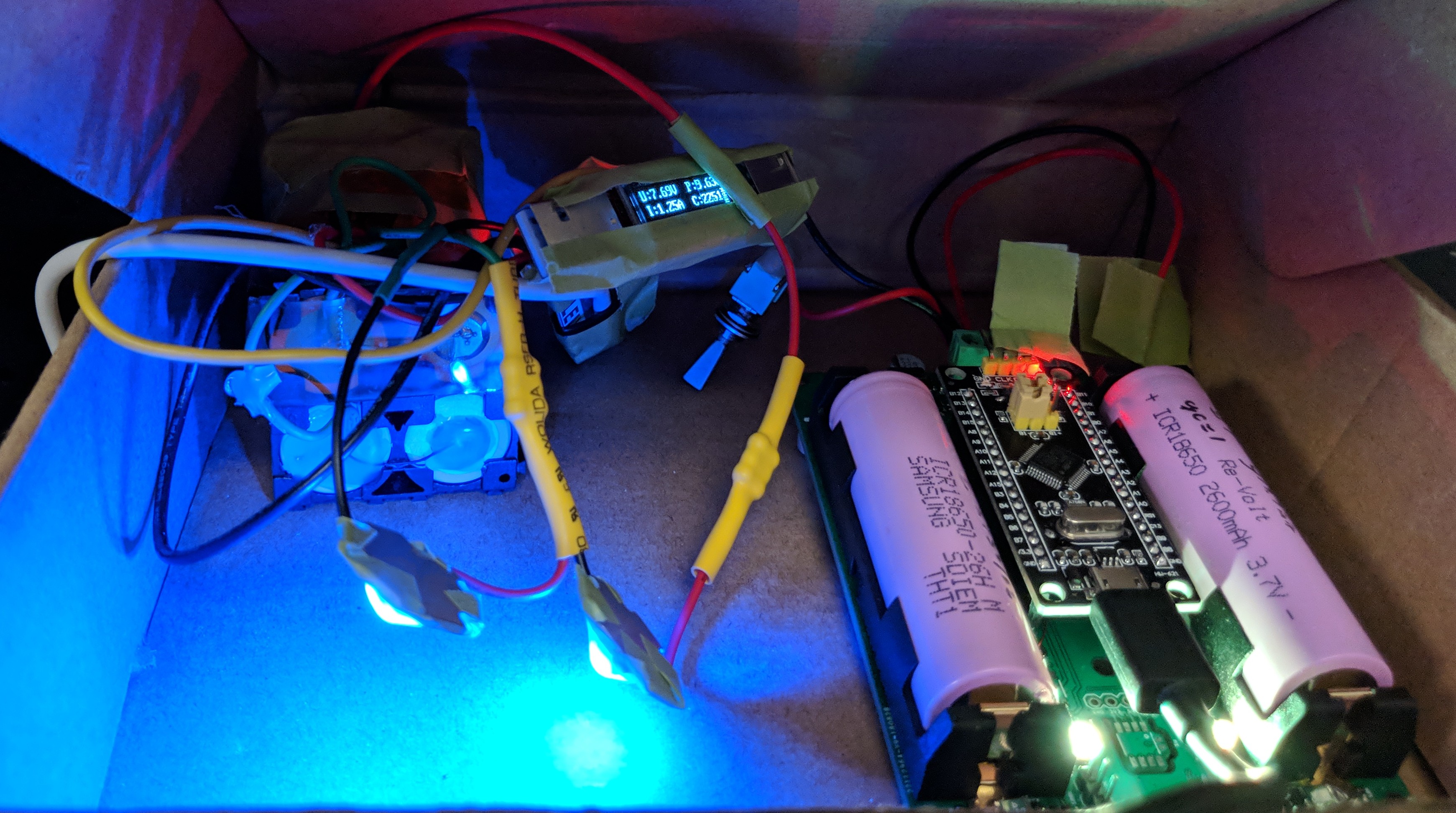
CCR v1 prototype in regenerative configuration
...

Total Project Cost
| EE Component | Cost | Source |
| OPA335 Zero-Drift Amplifier (qty 2) | $2.42 | LCSC |
| MCP1402 MOSFET Driver (qty 4) | $1.83 | LCSC |
| STM32F103 "Blue Pill" | $1.82 | Aliexpress |
| NCS199A1 Current Sense Amplifier (qty 2) | $1.45 | LCSC |
| 18650 SMT Holder (qty 2) | $1.23 | Aliexpress |
| N-channel MOSFET 13A 11.5mOhm SOIC-8 (qty 4) | $0.52 | LCSC |
| rBOM (under $0.41) | $4.76 | LCSC |
| PCB | $2.00 | JLCPCB |
| Assembly | $7.10 - $31.70 | PCBgogo |
| HW Component | Cost | Source |
| 100x40x20 Aluminum Heatsink | $3.02 | eBay |
| 40x40x20 5V Fan | $1.60 | eBay |
| Misc HW (Under $0.22) | $0.42 | Aliexpress/eBay |
| Total Price | $52.41 (Assembly cost $317, batch qty 10) |